


Topological insulators are characterized by zero electrical conduction within them, while currents with metallic character flow at their edges and surfaces. Moreover, in such currents, the spin of electrons, that is their property to rotate on themselves, shows a well-defined direction. This feature is of great interest among researchers in the field of spintronics, that branch of electronics that sees in the electron spin a fundamental resource to develop new devices for computation and information storage.
In fact, it is possible to use the so-called “spin-polarized” currents flowing on the surface of a topological insulator to manipulate the magnetic states of materials in contact with them and/or to carry “spin-dependent” information by exploiting their high conductivity, at a low energy cost. In this context, particular interest is directed to the optimization of the conversion between pure spin currents, i.e. without electric charge displacement, and conventional charge currents (and vice versa). These processes in fact guide the functionality of a wide range of innovative electronic devices, ranging from sensors and magnetic memories highly efficient and low power consumption, up to the development of complex architectures capable of simulating the operation of the nervous system.
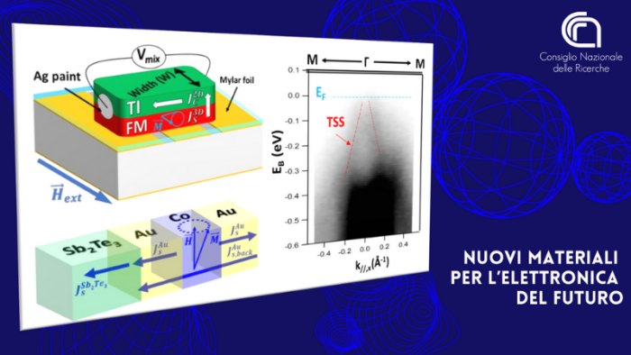
The studies conducted by researchers at the Institute for Microelectronics and Microsystems of the National Research Council (CNR-Imm) under the European project Skytop (https://skytop-project.eu), and published in Advanced Functional Materials and Advanced Materials Interfaces, have demonstrated a high efficiency of spin-charge conversion in antimony telluride (Sb2Te3), a topological insulator that has been “grown” through the technique of chemical vapor deposition metallorganic (Mocvd), already widely used in industrial contexts. The importance of the research is twofold. “On the one hand, we have developed spin-charge converters characterized by an efficiency comparable (and in some cases higher) to that reported to date in state-of-the-art systems based on topological insulators,” explains Roberto Mantovan, researcher at CNR-Imm.
“On the other hand, the use of the Mocvd technique has allowed us to optimize the production of topological insulators, the heart of such conversion processes, on silicon substrates having an area of several centimeters. And this is a fundamental requirement for bridging the gap between basic research and the technological transfer of these advanced materials in the electronic devices of the future, characterized by new functionalities, high performance and low energy consumption”.


